-
0 +Years of company establishment
-
0 +Foreign trade sales
-
0 +R & D personnel
-
0 +Patent certificate
Solutions
Solutions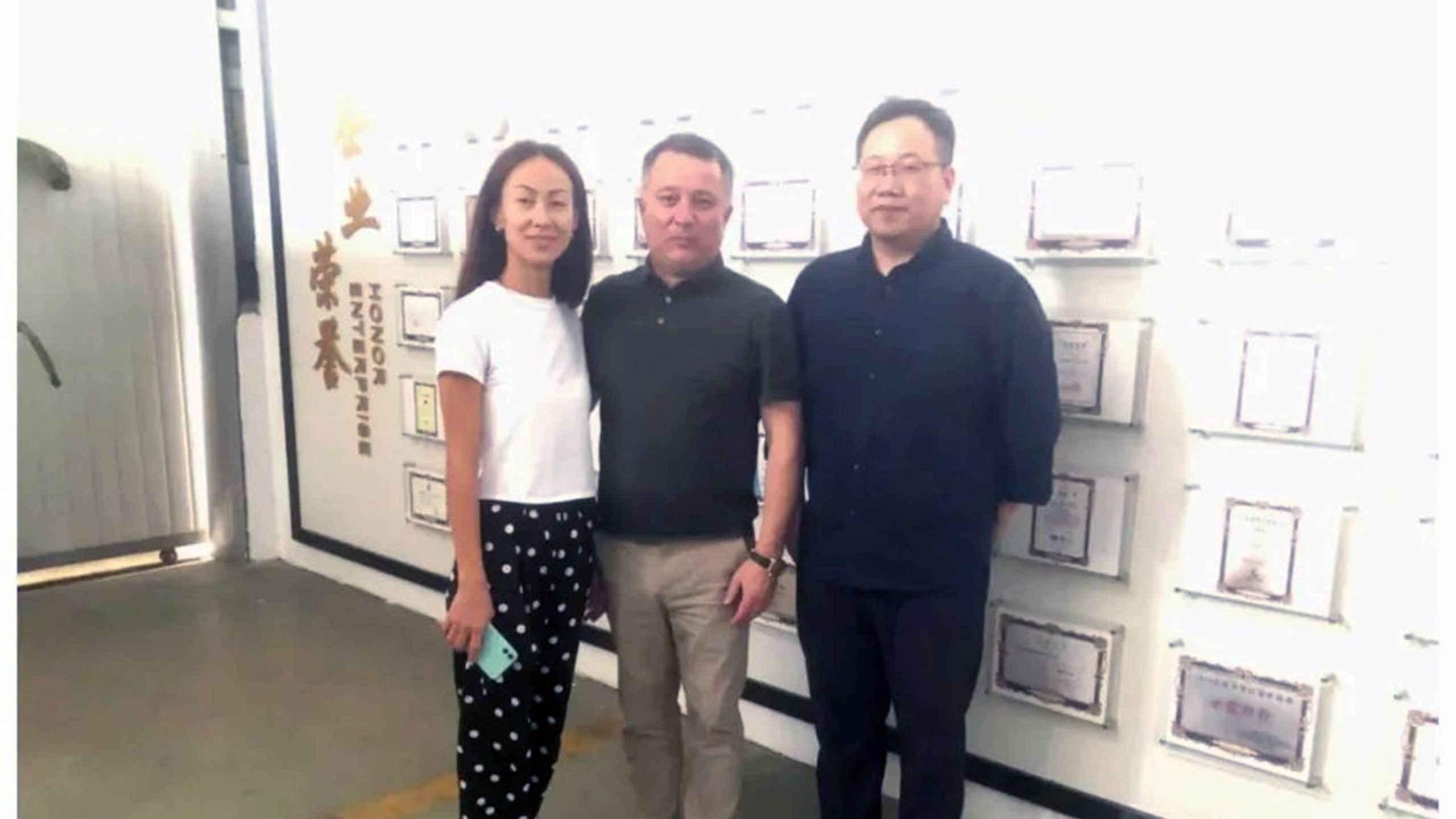


PRODUCT
PRODUCTABOUT US
ABOUT US
Founded in 2002, Huijue Networks is a high-tech service manufacturer integrating intelligent network communication equipment and an integrated application of computer intelligent network communication systems. The company is committed to becoming a leader in the network link industry. Headquartered in the Lingang New Area of Shanghai Free Trade Zone, with a registered capital of 107.78 million yuan, it currently has 6 wholly-owned subsidiaries across the country. Three production bases have been established in Fengxian, Jiangsu, Hai’an, Jiangsu, and Yangzhou, Jiangsu.
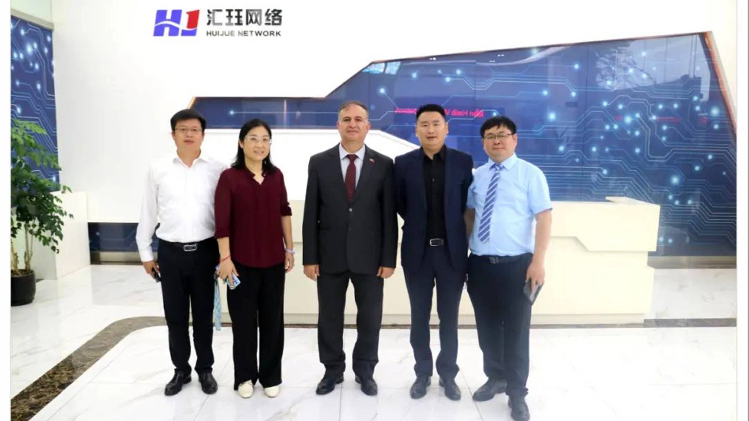
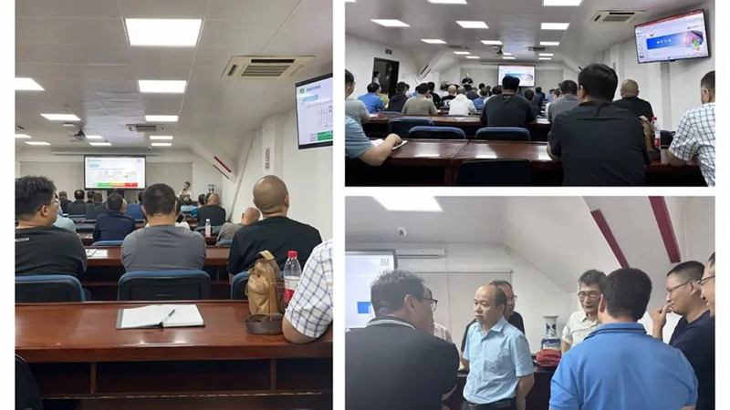
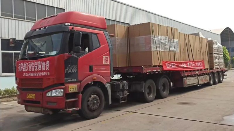
NEWS
NEWS
|
|